Thursday, December 29, 2022

Flying Pig Rig (7). Transmitter working

 I was very careful to install the finals correctly,  I read the instructions,  then checked the pinout of the BD139s on the data sheet, then....  then I managed to install them backwards anyway...

The board layout for this PCB is not the best in my opinion.  The holes are too small and the blank area between the pads and the ground plane is to narrow too.   With the small holes, it is impossible to use solder wick to desolder the holes.  The surface tension of the liquid solder holds the solder tightly in the hole and it's a real fight to desolder a part and get it out.  I managed to tear up a land going to one of the finals and had to solder a wire in to replace it. 

At power supply of 13.6 volts, the output to the 50 ohm dummy load is 12.2 volts RMS.  The waveform is shown below.   Power into the load is 3 W. 

After this I'll work on the cabinet.  Gonna make a simple 3D printed cabinet


Flying Pig Rig (6). Receiver checks

 Yesterday, I finished adding the last parts to the PigRig:  the lowpass filter inductors and a couple of more inductors.  I tested the receiver.  The AGC circuit was killing the mixer so I just disconnected it.  I kluged in the volume control and connected some headphones and a random wire antenna.   The receiver is fixed tuned at 7.030.7 kHz, but I heard some background noise and some faint CW signals. 

As it stands now,  I've wired around the keyer, which wasn't working right, and I've also disabled the AGC circuit. 

Next up is installing and checking the finals.  Then putting it into a cabinet.


Tuesday, December 27, 2022

Flying PigRig (5) -- Oscillator ok, keyer problems

 Link to PigRig schematic

Link to PigRig assembly instructions

At this point I am at Step 12 in the assembly instruction.  This step covers the winding and installation of remaining toroids.  The remaining steps involve installing the antenna lowpass filter toroids and L2, the inductance in the 12V power feeding the centertap of the finals. 

Before proceeding, I decided that this would be a good time to stop and test the low power circuits before proceeding to mess with the transmitter finals. 

Oscillator check

The oscillator works well, and voltages are in line with the table of oscillator voltages given in the instructions.  The trimmer capacitor C26 was bad, it jammed and wouldn't turn.  I replaced it with a capacitor from a trimmer assortment I bought a few months ago. 


The trace above is at the base of oscillator transistor Q4.  7.4 volt peak to peak. 

Keyer Ckt:

The keyer circuit consists of  a small ATtiny13A microcontroller programmed as a simple keyer chip. On powerup it defaults to a 15 wpm iambic keyer.   The circuit appears to be working except that the keying is modulated by pulses with 760 us period and about 10% duty cycle as shown below.   This is the "KEY" output of the keyer. 
I was thinking this is some kind of PWM signal but there's no integrator circuit that would convert the signal to an analog voltage.  I've put an inquiry on the 4 State mailing list about whether this pulsing is normal or not.  If I can find the source code to the keyer, I can check it to see if the pulsing is programmed in.  For now,  I guess I'll work around the problem

Checking U4 (keyer) pin 2, for the sidetone,  I get a square wave that's 641 Hz, which is within 3% of the nominal 625 Hz given in the instructions. 

The dot and dash intervals on the keyer KEY output are shown below, left and right respectively.  Notice the pulse modulation:


The dit interval is 74 ms, dah is 232 ms.  Using Farnsworth: 
$WPM = \frac{60}{50\cdot\tau_{dit}}=16.2 WPM$
which is close to the nominal 15 WPM in the instructions.  

For now I'm going to remove the keyer chip and wire a straight key from the drain of Q10 to ground.   I won't have a sidetone signal, but that's not a big deal.  

I'll test transmit stage 1 amp at it's input to T1, then move on to test the receiver.

Monday, December 26, 2022

Assembling PigRig (4) -- Schematic transcribed.

 I am planning to start testing the 40 meter PigRig that I have. The schematic provided with the assembly instructions is very crowded, making it difficult to understand the functions of the circuits.  As an exercise, I transcribed the schematic to KiCad and redrew the the circuits to show the unit's functional blocks.    The resulting PigRig schematic is in two pages, shown below.

Click each image to enlarge.  PDF copy of the schematic is located here. 


Thursday, December 22, 2022

20-Meter High Performance Direct Conversion Receiver (6) with update

I did some troubleshooting of a motorboating problem with the 20m direct conversion RX we've been working on.  We moved the RX and TX circuit boards to separate cabinets in get more room around the boards and to cut possible interference between the RX and TX wiring, especially for the antenna tuner and oscillator variable capacitor wiring.  We also install and modification from the TX QST article (Dec 1978). The mod, shown in the diagram below, cuts the connection that supplies power to  the RX preamp Q3. The supply lead is routed to the transmitter "RX MUTE" switch, which supplies 12V to the preamp when the RX operates and disconnects the supply when the RX MUTE is active.

The circuit had severe motorboating, which went away when I removed the RX MUTE mod.  I think we can run without the RX MUTE mod,  so I'm going to leave it without the mod for now.  Later we can add an RF choke and bypass capacitance to the RX MUTE line that would probably fix the motoboating. 

The RX has a lot of hum and noise, but I suspect that's due to my setup:  I don't have a real antenna or even a decent ground in for my workbench.  

A bigger problem is that the VFO drifts too much to follow CW signals.  There are two capacitors in the oscillator tank that I will replace with NPO caps, to see if that cures the problem. 

Dec. 23: diagnose oscillator drift.  Replace C19 and C20 with NPO caps.  
  • Drift is less severe
  • Lowest frequency is about 14.2 MHz, need to fix
Dec. 23: noticed that oscillator produces about 500 mV RMS, but according to LTSPICE model and QST schematic, amplitude should be 2 V RMS.  Changed out the oscillator transistor Q4 for another MPF102
  • Amplitude increased slightly to 600 mV RMS.  
  • Disconnected oscillator from mixer by removing C22.  Oscillator amplitude increased to 800 mV RMS.
  • Check 1N914 diode D1 forward voltage.  

QRP LABS 10W PA (1) MOSFET bias circuit

 I first mentioned the QRP LABS 10W power amplifier that we're working on in blog entry Loose Ends (1).   This QRP Labs power amplifier (PA) seems to be popular and there are several YouTube videos about the amp.  I watched a series of videos about this amp by NA5Y. Link here.  He goes into a detailed discussion of the amplifier's circuit which I found very interesting. 

The PA has an interesting bias compensation circuit for the first push-pull amplifier stage.  This PA 1st stage is shown in the bottom of the circuit below.  It consists of a pair of BS170 MOSFETs in a push-pull configuration. The bias for the FETs is supplied via the centertap on the secondary of T201. 

The bias circuit feeding the gates of Q203 and Q204 is temperature compensated, and, to me, the circuit seems both simple and elegant. It consists of Q202 and Q201 and associated resistors and diode, shown in the upper left of the diagram below. 

When power MOSFETs are operated as linear amplifiers, they are notoriously unstable with temperature. The FETs have a negative temperature coefficient for the threshold voltage. Being square-law devices the drain current is given as: 

$I_{DS} = K(V_{GS}-V_T)^2$  

Extracting some data from the Fairchild BS170 datasheet, $K = 78 mA/V^2$ and $V_T = 2.0 V$.

The threshold voltage temperature coefficient, extracted from the graph above, is 
$TC =-016$% per degC.  The circuit is designed for an idle current of 20 mA in each transistor. With a 12 volt power supply and 20 mA current, then each device dissipates about 240 mW.  The design temperature is 25C (77F).  Through a combination of elevated ambient temperature and operating inefficiency, let's say the junction  temperature is raised to 60C (140F).  In that case the threshold voltage will decrease from 2.0 volts to:

$V_T(60C) = 2.0V\cdot\left[1-(60C-25C)\cdot-0.0016\right] =1.89 V$

This increases the power dissipation in each transistor to 353 mW,  nominally exceeding the 350 mW datasheet rating of the BS170 transistor.   In practice, what happens is that power dissipated by the transistor raises the junction temperature of the transistor which lowers the threshold voltage which causes the dissipated power to increase, which raises the junction temperature....  This positive feedback loop is called "thermal runaway" and the cycle ends when the transistor is destroyed.

The bias supply circuit, taken from the schematic is shown below. 

VDD1 is the input voltage, assumed to be 12V, while VBIAS1 is the output of the circuit that sets the quiescent gate to source voltage of the amplifier transistors.   Let's redraw the circuit in a classis "foldback circuit"  configuration: 


Now we see that the circuit operates MOSFET Q202 as a DC current source, with negative feedback supplied by the Q201 NPN  transistor. We know that the silicon 2N3904 transistor, operating as a linear amplifier, will have a base emitter voltage of about  $V_{BE} = 0.65V$.   Given this the current in Q202 can be calculated: 

$I_{DS}=\frac{V_{BE}}{33\Omega}$

which works out to about 20 mA.   Now add the voltages from ground through R206 through the source to gate of Q202 and through diode D201 to VBIAS1 we get:

$VBIAS1 = V_{BE} + V_{GS}-V_D$

D201 and Q201 are both silicon devices so we know that 

$V_{BE} = V_D$     combining the two equations gives: 

$VBIAS1 = V_{GS}$

Now if Q202 is thermally connected to the two amplifier transistors, and the characteristics of all transistors match, then VBIAS1, supplied to the the amplifier transistors' gates, will produce the same quiescent current in those transistors as Q202.  So each amplifier transistor should have 20 mA quiescent current. 

If the temperature of the transistors goes up, the threshold voltage will decrease but Q201 will reduce VGS of Q202 to maintain Q202 drain current to 20 mA.  This reduced VGS will be reflected in VBIAS1, which will reduce the gate to source voltage of the amplifier transistors to maintain their quiescent current at 20 mA. 

As can be seen,  the bias circuit compensates for changes in transistor temperature and also makes the quiescent bias currents independent of the VDD1, the circuit supply voltage.   

For this circuit to function well however, the three MOSFETs have to have well-matched characteristics, and furthermore  their junction temperatures must track as well.  In practice, if the transistors all come out of the same bag from the manufacturer, then the characteristics usually match fairly well.  Using a curve tracer or some jig, the transistors can be selected manually to match. 

Temperature tracking is more problematic, since the TO-92 transistor package of the BS170 is not designed to transfer heat efficiently to a heatsink, but is designed to operate free standing in air.  This amplifier has a scheme to tie the three transistors to a common heatsink to match temperatures.  It will be interesting to investigate how well that scheme works. 


Wednesday, December 21, 2022

Tuna Tin S (9) Installing screw inserts in cabinet

 Still learning Fusion 360, a rocky experience, I designed a simple test block to practice putting M3 inserts in 3D printed cabinets for the Tuna Tin S. 

The inserts were ordered off Amazon  Here's a link. 

The test block is PLA material and consists of an array of 4 mm diameter holes in a 10 mm thick block. The infill is set to 20%, and the wall thickness set to 0.8 mm. 

I used a 10 Watt Ungar Princess model soldering iron.  According to Ungar's 1967 catalog it was newly introduced for microelectronic soldering at the time.  The heating element has, according to the catalog, has a tip temperature from 550F to 650F.  The soldering iron belonged to our grandmother, Ruth Chandler, who was an assembly worker at Dorsett Electronics in Tulsa in the 1970s.  So the iron is around 50 years old  ;-)  . 


I placed the insert tapered end outward on the tip of the soldering iron. 


I let the insert heat up for awhile, then inserted it into the hole of the test piece.  It sinks into the test piece gradually,  and I stopped when the top of the insert was even with the surface of the test piece.  Alignment doesn't seem to be much of a problem.  A recommendation from a YouTube video, linked here, is to stop inserting the insert when the top is just above the surface of the plastic, and then do final placement pushing the insert flush with a flat tool like a hammer's striking surface.   I tried that way and it worked well.  I also tried just doing the whole thing freehand and didn't see much difference in alignment.  The screws I used were 8 mm long M3 screws. 

The screw is driven by an Allen wrench.   I can exert quite a bit of torque, as shown in the photo below, and the insert holds without breaking the plastic.

I'm planning to use these M3 inserts, along with M2 inserts to design all 3D printed cabinets for projects going forward. 


Monday, December 19, 2022

First Fusion 360 project (2)

 As shown in the photo below. The scope bracket came out well after 12 hours of printing.  It's a tight fit however.  I designed the inner width dimension to clear the scope by 5 mm.  However when I added the sidewalls, I took away 6 mm of clearance without thinking about it.  There was still enough slop for the scope to fit it, but tightly.  I'll remember to check clearances carefully before printing next time.  "The burned hand teaches the best."  The 3rd photo below shows the scope installed under a shelf on my workbench.


Sunday, December 18, 2022

First Fusion 360 project

 I subscribed to the free version of Fusion 360 and started struggling through a tutorial. I've been using Sketchup for the last 10 years or so, since back when it was still owned by Google. 

Fusion 360 appears to be very sophisticated, intended as a professional solid modelling tool.  Looks to me like the learning curve is going to be kinda steep.  Let's see how it goes.

The project shown below is on the 3D printer right now.  It is a bracket to hold my TiePie Handyscope under a shelf on my workbench.  It's a 12 hour print, so it should be finished at about 10 am tomorrow morning. 


Friday, December 16, 2022

Fixing KY-040 rotary encoder problems interfacing to Wemos D1 Mini

 I am in the process of building  a version of AK3Y's Tuna Tin S, which is presented in December 2020's QST.  The attractiveness of the project is to replace old style VFO circuits with a low-cost digital synthesizer. I decided to use a Wemos D1 Mini clone for the synthesizer control, rather than the Arduino Nano shown in the QST article. I was able to get the D1 Mini, Si5351 synthesizer breakout, and the KY-040 rotary encoder going pretty quickly on a bread board.  

After building a second version wired on a PCB, I noticed that when rotating the encoder knob that the unit was counting frequency up and down erratically.   Upon investigation, I found that the encoder had a great deal of switch bounce that was causing misclocking of the counting algorithm in the controller.  The photo below shows the signal from the encoder CLK line transitioning from low to high with about 15 usec of switch bouncing. The switch bounce can cause havoc with the rotary encoder counting routine in the controller.  Misclocking caused by switch bounce tends to cause the counter to count erratically. 

I downloaded AK3Y's Nano program which is written in Arduino IDE, and ported this code over to the D1 Mini.  In the article and program,  the encoder CLK and DT lines are tied to digital input of the Nano.  The CLK falling edge  generates an interrupt.  The interrupt routine is shown below:  

There is some debounce code added to ignore interrupts that occur within 5 ms after a previous interrupt.  The frequency gets changed in the interrupt routine.  In the main loop if the frequency  changes (caused behind the scene during interrupt), then the synthesizer and display are updated with the new frequency.
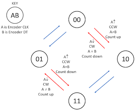
The principle of operation can be understood by examining the encoder state transition diagram. In the diagram below, the encoder CLK and DT are denoted A and B respectively in the state transition diagram. The encoder signals transition 00 to 10 to 11 to 01 to 00 when rotating clockwise and rotate 00 to 01 to 11 to 10 to 00 rotating counterclockwise.  When encoder CLK,  which is A, falls it corresponds to the transitions colored red in the diagram.  In the lower left, A (CLK) falls, and B (DT) is HIGH when the transition is finished.  This transition indicates a clockwise rotation and should generate a count upward. In the upper right transition, A (CLK) falls, and at the end of the transition B (DT) is LOW.  This transition is counterclockwise and should generate a count downward.  Looking at the interrupt code, which is entered immediately after the fall of encoder CLK, the routine checks DT.  If DT is LOW the frequency is decremented, otherwise the frequency is incremented. 


I ported this algorithm to the D1 Mini, but upon testing, the frequency counted erratically when the encoder was rotated.  I put the encoder up on the scope for diagnosis.  For trouble shooting purposes I added a test output of the D1 Mini.  This signal falls immediately after the DT is read in the interrupt routine and rises again immediately after the display and the Si5351 synthesizer are updated. I also added the 0.68 uF capacitor on the encoder CLK line. This capacitor is recommended in the AK3Y QST article.

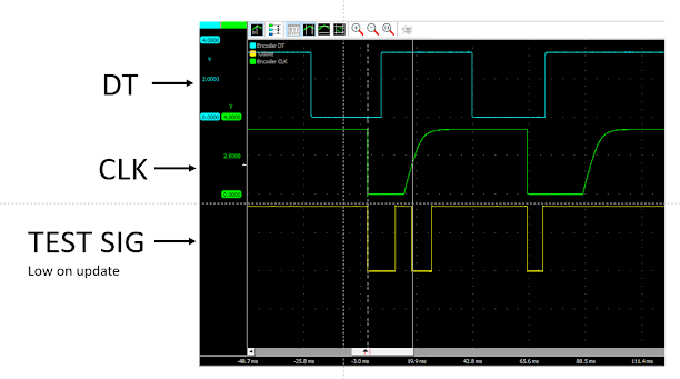
The resulting test signals are shown in the diagram below.  The encoder knob was turned two detents counterclockwise over a time interval of about 75 ms.  Note that when CLK (green curve) falls, the TEST SIG (yellow curve) goes low, indicating that the interrupt was triggered and the display and Si5351 were updated.   However the problem is that the rising edge of CLK also triggered an interrupt, as indicted by the fall of TEST SIG.  This is shown at the vertical white line in the diagram.  The interrupt pin is specifically setup to trigger on the falling edge of CLK, but often triggers on the rising edge as well. This causes erratic counting in response to turning the encoder knob.  
The false triggerings are probably a result of the slow rise of the CLK signal.  It is not good practice to drive digital inputs with slow moving signals.  The problem was repeatable and occurred using two different D1 Minis.  I did not try switching out to a different encoder.  It is possible that the Arduino Nano used by AK3Y didn't experience this false interrupt triggering. 

I did some more research and found some inspiration on the Components101.com site.  Follow the link and you'll find a KY-040 encoder datasheet and a good discussion of its construction and operation.  The test program included with the datasheet used a different algorithm for converting the encoder signals to counts. 

Observe the annotated encoder state diagram below.  Anytime CLK changes, whether rising edge or falling edge, we can determine the direction of rotation by observing whether the DT signals is the same as CLK, or whether DT is opposite of CLK.  In the first case the movement is counterclockwise and the count should be decremented, in the second case the movement is clockwise and the count should be incremented.  


I decided to abandon the use of interrupts and determine CLK transitions by polling. I also removed the capacitor off the CLK line. The loop section of the D1 Mini program is shown below.  After a check of the encoder push switch, the encoder service section begins at line 73.   If a check of the CLK signal shows a transition has occurred, then the encoder service routine is executed, otherwise the loop is begun again.  The encoder service is simple.  The DT signal is compared to CLK to determine the direction of rotation and the count (in this case a frequency variable) is incremented or decremented accordingly. After that, the display and the Si5351 are updated.  A diagnostic test output is toggled to indicate on the oscilloscope that the encoder service routine is active. 


The scope traces are shown below. In this case the encoder is rotating counterclockwise. As shown by the test signal, the encoder service routine is entered at every transition, up or down, of the CLK signal. After each transition CLK is always the same state of DT, so the count is decreasing as the knob rotates counterclockwise.  

Other tests at very fast time scale show that the latency for detecting a CLK transition by polling is less than 10 us.  This is sufficiently fast to avoid misreading the DT signal.  

Further the encoder service routine last about 6 ms before the routine returns to polling for a CLK transition again.  This is a sufficient delay to provide debounce of the encoder CLK signal.  The routine responds to the first valid transition in a bouncy transition and ignores other bounce transitions since it is away on the encoder service routine. 


Thursday, December 15, 2022

Loose Ends (1)

Here's a few things going on: 

1) Frequency Synthesizer.  I've been struggling with the code for the KY-040 rotary encoder in the frequency synthesizer.  I was trying to add switch debounce into the code, but this is much easier said than done.  The encoder is very noisy electrically, hence the need to debounce. But time for the fall of the CLK signal and the change of the DT signal is often just a couple of milliseconds... The DT line really needs to be sampled at the fall of CLK...   I'm running some experiments to characterize the problem, and will write a white paper on it later. 

2)  QRP LABS 10W amp.  I ordered a 10W linear amp from QRP Labs.  It apparently ships from Turkey.  It finally arrived yesterday.  The other QRP brother, KA5VZE, has promised to put the kit together for me.  We're going to drive the 10W amp with the frequency synthesizer to make a transmitter.  More on this later.  See photo below. 


3) The "Morris" Morse straight key:  I picked up the homemade "Morris" KA5VZE straight key yesterday.  It's awesome!  Now I just need a transmitter to plug it into...  
I want to customize it even more.  Maybe some idealized nose flames, or a mud flaps girl silhouette.. 

4)  Computer oscilloscope.  My bench oscilloscope is a Tek TDS2014.  It's fairly nice. 100 MHz bandwidth digital scope with 4 channels. The frustrating thing is that it doesn't have any way to offload digital data or even jpegs of the display.   I have an old TiePie Handscope HS4 lying around that I got from somewhere.  It's about 10 years old.  I'm going to try to get this going for the encoder study I'm planning.  This scope is displayed and controlled from a Windows computer.  The software is still available and I've downloaded it. Let's see if it works.  As I recall the scope had 100 ns, 12 bit sampling, and some huge buffer size. 


Monday, December 12, 2022

"Morris" key (6): qso with KD4RAX


Trying out Steve's "Morris" key on the 40 Mtr band with Mike @ KD4RAX.


Tuna Tin S (8). Cabinet Version 2

Son Sam sent a corrected stl file and I printed it out and mounted the board to it.  See photo below.
Everything lines up well now. Just a couple of adjustments needed. 
Below shows the alignment of the front panel parts.  Pretty good. 

Below shows view from the rear.  Mount screws go in well.


Sunday, December 11, 2022

Tuna Tin S (7), 1st try cabinet

Here's the first try on the cabinet. My son Sam and I designed it on Fusion 360, and I printed it out on my 3D printer.  See the photo below. The hole for the encoder was located in the wrong place. As can be seen,  I opened the encoder opening up with a nibbling tool.  The back view is below

The PCB is pushed forward to lock into slots behind the front panel, and two mounting screws at the back corners hold the PCB down. I didn't leave enough room under the PCB for the wiring, so we'll have to increase the dimension.  I used M4 machine screws as self tapping screws and they seem to do the job.  We'll try the corrected version tomorrow. 


Tuna Tin S (6), Wired up, ready to test.

 Finally got the synthesizer board wired up and checked.  The 1st photo show the board top side. 

The second photo shows the board underside.  The wiring was done with 28 AWG wirewrap wire, soldered pin to pin. 

The next task will be to design a box for it and get it mounted.  I need to check the power supply draw and maybe add some power supply filtering.   Presently, everything is powered through the D1 Mini USB connection.  The USB supplies 5V and the D1 Mini had a 3.3V regulator that supplies the ESP8266 controller and the other components in the unit: 1) OLED display, 2) Si5351 synthesizer, 3) rotary encoder.

I have a 10W linear amplifier on order from QRP Labs.  It's on it way from Turkey.  When it comes in we'll put it together and then drive it with this synthesizer and try some 40meter QRP activity.


Saturday, December 10, 2022

Tuna Tin S (5), Component placement & schematic

 I have populated the PCB for the Tuna Tin synthesizer, see the photo below.  I considered crowding the components more and cutting off the excess PCB area, but will just use this roomy component layout for adaptability.  Also I'm using this board for learning and practice.   See the photo below. 


I constructed the schematic to use when I wire the board.  See the diagram below. The schematic was entered using KiCad.  I had to construct symbols for the graphic dispay, the encoder, and the Si5351 breakout module. I'll need to add a 5V to 3.3 supply at some point, but for now it's being powered through the D1 Mini's USB port. 


Building a 1920s Tube Amplifier (And Tubes!)

Friday, December 9, 2022

"Morris" key (5): Boring the return spring recess with homebrew faceplate

In order to turn the recess that seats the return spring I had to devise a way of mounting the base onto the lathe in order to bore it out.  I drilled four holes in the back of a 3/4" thick disc for the 4-jaw chuck to have a purchase on it.  Once it was mounted on the lathe I leveled off the faceplate with a couple of passes of the cutting tool.  

 I then screwed the base onto the faceplate after centering it to the boring tool.  The streak across the base is where I forgot to manually turn the chuck to see it it interfered with anything.  And sure enough it did.  The carriage caught one of the screws used to mount the base and subsequently pulled the tool into the work.  Now it has a decorative element that is quite lovely,... Don't you think? It should buff out. :)

Old crystals

 At one time, back about 1987, I was busy building both QRP transistor rigs and replicas of vintage home brew projects. 

I often operated a Viking Adventurer as my transmitter. It was crystal controlled and had 50 watts input to the final tube. 


As my receiver at the time I had an old BC-342, an old Army receiver from the WWII era. I added a digital frequency counter to the BC-342.  It was made of 7400 series TTL logic a set of binary thumbwheel switches that I used to subtract the IF frequency from the oscillator frequency to get the actual receive frequency.   I designed that counter myself and spent four or five days at the kitchen table wire wrapping the circuit board.  

Anyway,  recently came across a handful of FT-243 crystals that I had ordered to use with my Viking Adventurer and with my experimental transmitters.  I ordered them from an outfit called CW Quartz Crystals in Marshfield, Missouri, in 1987.  So they are 35 years old.  The adhesive on all the labels had dried out and the frequency labels had all fallen to the bottom of the bin.  I had to spend a couple of hours with a signal generator and an o-scope, finding each crystal's resonant frequency and then reattaching the appropriate label.  

I was working on 80 meters and 40 meters and also experimenting with 30 meters, which explains the frequencies used.  There is only on 40 meter crystal left.  I must have lost the rest of the 40 meter crystals here and there as I moved around in the '90s.  

Thursday, December 8, 2022

Tuna Tin "S" (4), RF synthesizer, move to PCB

I've come to the point where I need to move the RF synthesizer to a PCB.  I am going to mount the encoder, D1 Mini, OLED, and Si5351 board all on a 60mm by 80 mm board.  I'll put the display and encoder on one edge to interface with the operator through a box wall.  I'm going to 3d print the box later,  but I'm considering a shielded metal box, or something made out of clad PCB panels. 

The photo below shows the candidate PCB.  I got the PCB from an assortment sold on Amazon.com Link  I still have to add a 3.3 volt power supply to the circuit.  For this I'll need to measure the total current draw of all the components.